Qualcomm Interview Prep — 09. Computer Architecture & Digital Design¶
Scope. This file owns the machine itself: how numbers are represented (signed/unsigned, two's complement ranges, number-system conversions, IEEE-754 floats), the memory hierarchy (registers→cache→RAM→disk) and cache organization, computer organization (CPU/ALU/control/registers/IO/buses block diagram), instruction pipelining and hazards, ISA RISC vs CISC, bandwidth vs latency, and the digital-design layer — combinational vs sequential logic, gates & Boolean/K-map simplification, MUX/decoder, latch vs flip-flop, setup/hold/propagation timing & max clock, finite-state machines (Moore/Mealy), metastability & clock-domain crossing, and Verilog/SystemVerilog RTL basics. It closes with how all of this maps onto ISP-architecture / pipeline-timing roles. Overlaps are cross-linked, not duplicated: bit-level C semantics, endianness,
struct/padding, and the program memory map live in01_c_programming.md; virtual memory / paging / MMU / TLB / context switches in04_os.md; the ISP image pipeline itself (demosaic→3A→tone-map) in05_camera_isp_multimedia.md; CPU/GPU/DSP from a kernel/driver angle in07_embedded_linux_kernel.md; C++ in02_cpp_oop.md; DSA/complexity in03_dsa.md; ML in06_ml_deeplearning.md; puzzles/number tricks in08_logical_puzzles_aptitude.md; LLD/system design in10_lld_system_design.md; behavioral in11_behavioral_hr_projects.md.How to read each entry. Every question is answered in layers so you can stop at the depth you need: - Q — the question, phrased as interviewers actually ask it. - Frequency — how often it showed up in the 75 collected reports (tier + approximate count). - Concept — the basis — book-style fundamentals with worked examples and, where it helps, an SVG diagram. - The "wh"s — Why it exists (what problem the feature/rule solves), Where you see it (real Qualcomm/camera/ISP/SoC situations), and any important caveat. - Answer — a tight, say-it-out-loud interview answer. - Solution / good example — for "how do you design/implement/handle X" questions, a complete, copy-pasteable RTL/code/design. - Follow-ups / gotchas — the traps interviewers spring next. - Seen in — the source reports.
Terms in bold-italics like two's complement, cache line, pipeline hazard, setup time, metastability, RISC are defined in the § Encyclopedia at the bottom — search there for any keyword.
Frequency legend (sample = 75 collected interview reports; counts are approximate and partly from aggregator pages, so treat them as directional): 🔥🔥🔥 Very common (~8+ reports) · 🔥🔥 Common (~4–7) · 🔥 Occasional (~2–3) · ◽ Foundational (rarely asked verbatim, but assumed and underpinning everything else).
Why architecture & digital design matter at Qualcomm. Qualcomm is a chip company — Snapdragon SoCs fuse CPU (Kryo), GPU (Adreno), DSP (Hexagon), ISP (Spectra), and modem on one die. Even pure-software camera roles are quizzed on memory hierarchy, cache, endianness and pipelining because performance lives there; and the Camera/ISP Architecture and ASIC/DV loops explicitly probe "digital-design fundamentals, timing constraints, pipeline architectures, and potentially HDL/RTL" (Blind/Reddit B2/B6). The screening test for several India loops has a dedicated Computer Architecture section. Evidence base: qualcomm_camera_interview_experiences.md.
Table of contents¶
- A. Number representation — A1 signed vs unsigned & two's complement · A2 number-system conversions (bin/hex/oct) · A3 IEEE-754 float layout & precision · A4 multiply/divide without the operator (bit tricks)
- B. Memory hierarchy & caches — B1 the memory hierarchy & locality · B2 why cache exists / cache functionality · B3 cache organization (direct/set-assoc/fully) · B4 write-back vs write-through & replacement · B5 cache coherence · B6 bandwidth vs latency
- C. Computer organization — C1 block diagram of a computer · C2 buses · C3 ISA: RISC vs CISC · C4 what happens when you press a key (HW→OS→CPU)
- D. Pipelining — D1 the 5-stage pipeline & hazards · D2 branch prediction
- E. Combinational & sequential logic — E1 combinational vs sequential · E2 gates & Boolean/K-map simplification · E3 MUX & decoders · E4 latch vs flip-flop / the D-FF
- F. Timing & FSMs — F1 setup/hold/propagation & max clock · F2 metastability & clock-domain crossing · F3 finite state machines (Moore vs Mealy)
- G. RTL & relevance — G1 Verilog/SystemVerilog basics (always blocks, blocking vs non-blocking) · G2 relevance to ISP-architecture / pipeline-timing roles
- § Encyclopedia — searchable glossary
- § Last-5-minutes cheat sheet
A. Number representation¶
A1 · Q: Signed vs unsigned integers and two's complement — give me the representation and the ranges.¶
Frequency: 🔥🔥 Common (~4 reports) — explicitly a "Computer Organization/Architecture: signed and unsigned integer ranges" question (Embedded System loop), and assumed everywhere bit-manipulation appears.
Concept — the basis. A fixed-width n-bit integer is just a bit pattern; the encoding decides what value it means.
- Unsigned uses all n bits for magnitude: range 0 … 2ⁿ − 1, arithmetic is modulo 2ⁿ (wraparound is well-defined).
- Signed almost universally uses two's complement: the most-significant bit has negative weight −2ⁿ⁻¹, the rest positive. Range −2ⁿ⁻¹ … 2ⁿ⁻¹ − 1 — asymmetric (one extra negative value). To negate: invert all bits and add 1.
8-bit examples (n = 8):
 unsigned:   0000_0000 = 0      1111_1111 = 255          range 0 … 255
 two's-comp: 0000_0000 = 0      0111_1111 = +127         range −128 … +127
             1000_0000 = −128   1111_1111 = −1
 negate +5:  0000_0101 → invert 1111_1010 → +1 → 1111_1011 = −5  ✓
int8 −128…127 · uint8 0…255 · int16 −32768…32767 · int32 −2,147,483,648…2,147,483,647 · uint32 0…4,294,967,295 · int64 ≈ ±9.22×10¹⁸.
Why two's complement (and not sign-magnitude or one's complement). It has a single representation of zero (sign-magnitude has +0 and −0), and — the killer feature — the same adder hardware does signed and unsigned add/subtract with no special sign logic: a − b is just a + (~b + 1). Carry-out is ignored; the result is automatically correct mod 2ⁿ. That hardware economy is why every modern CPU/ALU uses it.
Where you see it (Qualcomm). Pixel/sample values are unsigned (uint8_t, uint16_t for 10/12-bit raw stored in 16); image sizes and strides are size_t (unsigned); register fields are unsigned bit-patterns; signed deltas appear in motion vectors, gain/offset, and "difference of two timestamps." The classic ISP bug: subtracting two uint8_t pixels and storing the result back into a uint8_t — it wraps to a large positive (the subtraction itself promotes the operands to int, so the truncation on store is what wraps; keep the difference in a signed type).
Answer. "An n-bit unsigned integer covers 0 to 2ⁿ−1 and wraps modulo 2ⁿ. Signed uses two's complement: the top bit carries weight −2ⁿ⁻¹, range −2ⁿ⁻¹ to 2ⁿ⁻¹−1, so it's asymmetric with one extra negative. Negate by inverting bits and adding one. Two's complement wins because it has a single zero and lets one adder handle both signed and unsigned. So int8 is −128…127, uint8 0…255, int32 ≈ ±2.1 billion, uint32 0…~4.29 billion."
Follow-ups / gotchas. In C, signed overflow is undefined behavior; unsigned wrap is defined (full detail and the (-1 > 1u) mixed-comparison trap → 01_c_programming.md F2). INT_MIN has no positive counterpart (-INT_MIN overflows). Right-shifting a negative signed value is implementation-defined (usually arithmetic shift, sign-extending). Sign-extension vs zero-extension when widening matters when reading registers.
Seen in: GfG Embedded System ("Computer Organization/Architecture: Signed and unsigned integer ranges"); GfG FTE on-campus (endianness/representation block); cross-ref 01_c_programming.md F2.
A2 · Q: Convert between binary, hexadecimal, octal and decimal.¶
Frequency: ◽ Foundational — implicit in every register/bit question, the aptitude section, and any "reverse the bits / count set bits" problem.
Concept — the basis. A positional number in base b is Σ dᵢ·bⁱ. Conversions:
- Hex ↔ binary: each hex digit = exactly 4 bits (a nibble). Group binary in 4s. 0xB = 1011.
- Octal ↔ binary: each octal digit = 3 bits. Group in 3s from the right.
- Decimal → any base: repeated division, read remainders bottom-up.
- Any base → decimal: Horner / weighted sum.
Convert 0x2F to decimal & binary:
  0x2F = 2*16 + 15 = 47
  hex 2 = 0010, hex F = 1111  →  0010 1111  (binary)
  octal: 47 = 057  →  101 111 → 0b101111 ✓ (groups of 3: 101=5, 111=7)

Decimal 47 → binary by division:
  47/2=23 r1 | 23/2=11 r1 | 11/2=5 r1 | 5/2=2 r1 | 2/2=1 r0 | 1/2=0 r1
  read bottom-up: 101111  ✓
Why it exists / why hex. Binary is how hardware thinks but is unreadable for humans (0b00101111); hex is a compact stand-in because a byte is exactly two hex digits and a 32-bit register is exactly 8 — so register maps, addresses, and bitmasks are always written in hex. Octal survives mainly in Unix file permissions (chmod 755) because 3 bits = one rwx triad.
Where you see it (Qualcomm). Register addresses (0x4000_1000), bit-field masks (#define EN_BIT 0x08), MIPI/raw pixel-format codes, color values (0xFF00FF), and reading hex dumps of frame buffers/packets during bring-up.
Answer. "Hex digit = 4 bits, octal digit = 3 bits, so I group binary into nibbles for hex or triads for octal. Decimal-to-base is repeated division reading remainders bottom-up; base-to-decimal is the weighted positional sum. Hex dominates in hardware because one byte is two hex digits and a 32-bit word is eight, matching registers and masks cleanly."
Follow-ups / gotchas. Watch prefixes: 0x hex, 0 (leading zero) octal in C — 010 == 8, a real bug source. Two's-complement negatives in hex: −1 as uint32 is 0xFFFFFFFF. To check "power of 2" use n && !(n & (n-1)) (asked repeatedly — see A4 / cross-ref 03_dsa.md bit tricks).
Seen in: Aptitude/programming sections across GfG OAs; underpins "reverse the bits of a number", "count set bits", "power of 2" (GfG Set 8, ML&System, exp 16/18).
A3 · Q: Explain the IEEE-754 floating-point format — single and double — and its precision limits.¶
Frequency: 🔥 Occasional / commonly expected — aggregator-reported as a core "computer architecture" topic; floats underpin ISP gain/tone-curve math and ML.
Concept — the basis. A float stores a number in binary scientific notation (−1)ˢ × 1.f × 2^(E−bias), packed into three fields:
| Format | Total | Sign | Exponent | Fraction (mantissa) | Bias | ~Decimal digits |
|---|---|---|---|---|---|---|
Single (float) |
32 bits | 1 | 8 | 23 | 127 | ~7 |
Double (double) |
64 bits | 1 | 11 | 52 | 1023 | ~15–16 |
The leading 1. is implicit (not stored) for normalized numbers — you get 24 bits of significand "for free" from 23 stored. The exponent is biased (stored = actual + bias) so the field is an unsigned value yet represents negative exponents, which makes float comparison reduce to integer comparison of the bit pattern.

Encode −6.5 as a single-precision float:
  6.5  = 110.1₂ = 1.101 × 2²
  sign S = 1 (negative)
  exponent E = 2 + 127 = 129 = 1000_0001
  fraction = 101 followed by 20 zeros
  bits: 1 1000_0001 101_0000_0000_0000_0000_0000  = 0xC0D00000
Why it exists. Fixed-point can't span the huge dynamic range science/graphics need (10⁻³⁸ to 10³⁸ for single) with a fixed bit budget. Floating point trades uniform absolute precision for uniform relative precision — more resolution near zero, coarser for large magnitudes — which matches how physical quantities scale. IEEE-754 standardized the bit layout, rounding modes, and ∞/NaN so results are portable and reproducible across vendors.
Where you see it (Qualcomm). ISP tuning math (gains, gamma/tone curves, color-correction matrices) often runs in float on a DSP/CPU before quantizing back to fixed-point for the hardware; ML/CV weights (FP32 training, FP16/BF16/INT8 inference on Hexagon NPU); GPU shader math. Knowing FP16's tiny range/precision explains why quantization-aware training and careful scaling matter.
Answer. "IEEE-754 stores (−1)^sign × 1.mantissa × 2^(exponent−bias). Single precision is 1 sign + 8 exponent (bias 127) + 23 fraction = 32 bits, ~7 decimal digits; double is 1 + 11 (bias 1023) + 52 = 64 bits, ~15–16 digits. The leading 1 is implicit for normalized values, the exponent is biased so the field stays unsigned, and reserved exponents give ±0, subnormals, ±∞, and NaN. Precision is relative, so large numbers lose absolute resolution and values like 0.1 aren't exact — which is why you never compare floats with ==, you use an epsilon."
Follow-ups / gotchas. 0.1 + 0.2 != 0.3 exactly (binary can't represent 0.1) — compare with fabs(a-b) < eps. NaN != NaN (use isnan). Catastrophic cancellation when subtracting near-equal floats. FP16: 1+5+10 bits, bias 15, max ≈ 65504 — overflows easily. BF16: 1+8+7, same range as FP32 but fewer mantissa bits — popular for ML because it just truncates FP32.
Seen in: Commonly-expected computer-architecture topic (GfG "IEEE-754" architecture material); relevant to ML float facts in 06_ml_deeplearning.md (FP16/BF16/INT8 quantization).
A4 · Q: How would you multiply (or divide) two numbers without using the * (or /) operator?¶
Frequency: 🔥 Occasional (~2 reports) — "if you want to multiply two numbers, how would you do it (discuss many approaches)" (kernel SWE loop); "divide a number by 4 without the division operator" (SDE loop).
Concept — the basis. Multiplication and division by powers of two are bit shifts; general multiply is shift-and-add (the schoolbook algorithm in base 2), exactly how a hardware multiplier works.
- x * 2ᵏ = x << k; x / 2ᵏ = x >> k (for unsigned; signed >> rounds toward −∞, not 0).
- General a * b = sum of a << i for every set bit i of b.
/* multiply via shift-and-add (works for unsigned; handle signs separately) */
unsigned mul(unsigned a, unsigned b){
    unsigned res = 0;
    while (b) { if (b & 1) res += a; a <<= 1; b >>= 1; }
    return res;
}
/* divide by 4 without '/' : just shift right by 2 (unsigned) */
unsigned div4(unsigned x){ return x >> 2; }      /* x / 4 */
/* multiply by 10 = (x<<3) + (x<<1)  i.e. 8x + 2x */
int mul10(int x){ return (x << 3) + (x << 1); }
Why it's asked. It's a fast, unfakeable probe that you (1) think in binary, (2) know shifts equal power-of-two multiply/divide, and (3) understand the signed-shift caveat. It mirrors how the ALU and the compiler's strength reduction optimization actually replace *// by shifts.
Where you see it (Qualcomm). DSP/ISP kernels avoid expensive divides — gain by 2ⁿ, downscale by >>1, address arithmetic, fixed-point Q-format scaling. A divide costs many cycles; a shift costs one.
Answer. "Multiply/divide by a power of two is a left/right shift. For general multiply I'd do shift-and-add: for each set bit i of one operand, add the other shifted left by i. Divide by 4 is x >> 2 for unsigned. The catch is signedness — arithmetic right shift of a negative number rounds toward negative infinity, not toward zero, so -7 >> 1 is -4, not -3; the compiler adds a bias for signed division. This is exactly the strength-reduction the compiler does automatically."
Follow-ups / gotchas. Signed / truncates toward 0 but >> floors — they differ for negatives. Overflow during shifting. "Power of 2 check": n > 0 && (n & (n-1)) == 0. "Swap without temp": XOR trick a^=b; b^=a; a^=b; (but the temp version is clearer/faster — interviewers accept either; cross-ref 03_dsa.md).
Seen in: LeetCode kernel SWE ("multiply two numbers, many approaches"), GfG SDE off-campus ("divide a number with 4 without division operator"), GfG on-campus ("swap two numbers without a third variable").
B. Memory hierarchy & caches¶
B1 · Q: Explain the memory hierarchy and the locality principle that justifies it.¶
Frequency: 🔥🔥🔥 Very common (~8 reports) — "memory hierarchy / cache memory / CPU functions" (System SW round), "memory hierarchy ordering: main memory, secondary memory, cache — proximity to processor" (Embedded System), "different types of memories present in a computer" (FTE on-campus), "cache, RAM, secondary memory speed comparison" (off-campus 2021).
Concept — the basis. No single memory is simultaneously fast, big, and cheap, so machines stack several, fastest/smallest at the top:
| Level | Typical latency | Typical size | Managed by |
|---|---|---|---|
| Registers | ~0 cycles | ~KB (32–64 GP regs) | compiler/ISA |
| L1 cache (split I+D) | ~1–4 cycles | ~32–64 KB/core | hardware |
| L2 cache | ~10–14 cycles | ~256 KB–1 MB/core | hardware |
| L3 / LLC (shared) | ~30–40 cycles | a few MB | hardware |
| Main memory (DRAM/RAM) | ~100–300 cycles (50–100 ns) | GBs | OS (virtual memory) |
| Secondary (SSD/flash/disk) | ~10 µs – 10 ms | GBs–TBs | OS/filesystem |

The whole scheme only works because real programs exhibit locality of reference: - Temporal locality — a byte used now is likely used again soon (loop counters, hot variables) → keep it in fast memory. - Spatial locality — bytes near one just used are likely used soon (array traversal, instruction streams) → fetch a whole cache line (e.g. 64 B), not one byte.
Why it exists. Physics and economics: SRAM (cache) is fast but expensive and power-hungry; DRAM is denser/cheaper but slower; flash/disk is cheapest per byte but far slower. Putting a small fast cache in front of large slow memory gives most of the speed of SRAM at most of the capacity/cost of DRAM — because locality means the small cache catches the vast majority of accesses (high hit rate).
Where you see it (Qualcomm). Per-pixel ISP/DSP loops are tuned so a frame's working set fits in cache; row-major image traversal exploits spatial locality (walk pixels along the cache line, not down columns); DMA streams frame data so the CPU isn't stalled on DRAM; tightly-coupled memory (TCM) on the Hexagon DSP is a software-managed fast scratchpad. The classic interview line: caches are the reason a cache-friendly loop is 10× faster than a cache-hostile one with identical instruction count.
Answer. "Memory is layered because nothing is fast, big, and cheap at once. From the top: registers (~0 cycles), L1 (~1–4), L2 (~10), L3 (~30–40), DRAM (~100s of cycles / tens of ns), then SSD/disk (microseconds to milliseconds) — each step bigger, slower, cheaper per byte. It works because of locality: temporal (reuse the same data soon) and spatial (use nearby data soon), so a small fast cache near the CPU captures most accesses. That's why we fetch whole cache lines and write cache-friendly, row-major loops."
Follow-ups / gotchas. Order of proximity to processor: registers → L1 → L2 → L3 → RAM → disk (a literal exam question). AMAT (average memory access time) = hit time + miss rate × miss penalty — the formula that motivates everything. Don't confuse the cache hierarchy (hardware) with virtual memory (OS-managed RAM↔disk paging → 04_os.md).
Seen in: Medium System SW (exp 16, "memory hierarchy, cache memory, CPU functions, cache coherence"), GfG Embedded System (exp 41, memory hierarchy ordering), GfG FTE on-campus (exp 19, "types of memories… cache working, cache types, LRU"), GfG off-campus 2021 (exp 44, "cache, RAM, secondary memory speed comparison").
B2 · Q: Why do we use cache memory? What does the cache do?¶
Frequency: 🔥🔥 Common (~4 reports) — "Why do we use Cache Memory?" and "What is Cache Memory in Computer Organization?" (FTE on-campus, Technical Profiles), "cache functionality" (off-campus 2021).
Concept — the basis. A cache is a small, fast SRAM buffer between the CPU and main memory that holds recently/soon-to-be-used data and instructions. On every memory access the cache is checked first: - Hit — data is present → served in a few cycles. - Miss — data absent → fetch the whole cache line from the next level (paying the miss penalty), install it, then serve. Future accesses to that line hit.
The payoff is quantified by AMAT = hit_time + miss_rate × miss_penalty. With a 95% hit rate, a 2-cycle hit and a 200-cycle miss penalty, AMAT ≈ 2 + 0.05×200 = 12 cycles — versus 200 for every access without a cache.
Why it exists. The processor–memory gap: CPU clocks raced ahead of DRAM latency for decades, so a load from DRAM can cost hundreds of cycles — the CPU would stall, starved for data/instructions. Cache bridges that gap by exploiting locality (B1): keep the small hot working set close, so the slow DRAM trip is rare.
Where you see it (Qualcomm). Real-time camera/codec pipelines must hit frame deadlines; a cold cache or cache thrashing on a per-frame loop blows the budget. Engineers profile cache misses, tile image processing so a tile fits in L1/L2, prefetch the next row, and align/pack data to lines. On the hardware side, ISP/DSP blocks have their own line buffers/SRAM for exactly this reason.
Answer. "Cache is fast SRAM that sits between the CPU and slow DRAM and holds recently and nearby-used data. It exists to close the processor–memory gap: a DRAM access costs hundreds of cycles, so without a cache the CPU stalls constantly. On a hit you save the trip; on a miss you fetch a whole line and benefit from locality afterward. Average access time is hit time plus miss rate times miss penalty, so even a 90–95% hit rate slashes effective latency by an order of magnitude."
Follow-ups / gotchas. Three miss types (the 3 Cs): Compulsory (first-ever access / cold), Capacity (working set bigger than cache), Conflict (too many lines map to the same set — fixed by more associativity). Bigger cache → fewer capacity misses but slower hit time and more power. Cache pollution from a one-shot streaming pass (non-temporal stores help). The cache stores lines, not bytes — false sharing across cores is a multicore pitfall.
Seen in: GfG FTE on-campus (exp 18, "Why do we use Cache Memory?"), GfG Technical Profiles (exp 24, "Cache Memory in Computer Organization"), GfG off-campus 2021 (exp 44, "Cache functionality"), Medium System SW (exp 16).
B3 · Q: Explain cache organization — direct-mapped vs set-associative vs fully-associative. How does an address map to a line?¶
Frequency: 🔥🔥 Common (~4 reports) — "cache types" / "cache working" (FTE on-campus), follow-ups to every cache question; explicit on the ISP-architecture loop.
Concept — the basis. Main memory is divided into blocks the size of a cache line (e.g. 64 B). The cache decides where a given memory block may sit. The physical/virtual address is split into three fields:
| ---- TAG ---- | -- INDEX -- | -- OFFSET -- |
   identifies      selects       byte within
   the block       the SET       the line
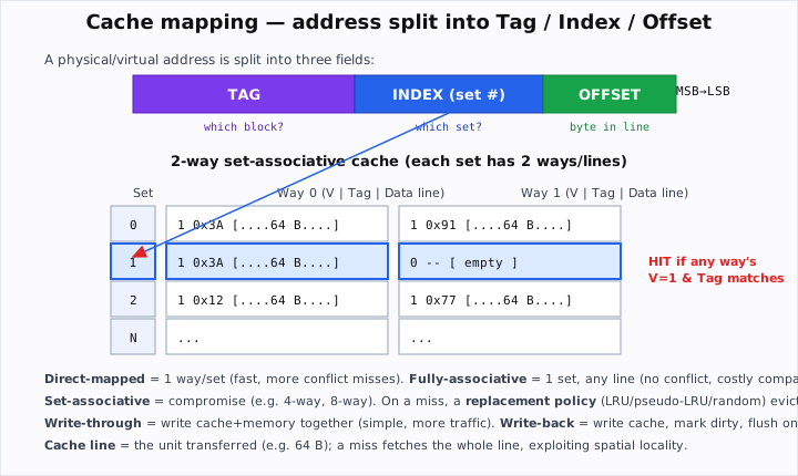
Three organizations differ in how many lines a block can occupy:
- Direct-mapped (1 way/set): each block maps to exactly one line (index = block# mod #lines). Fast, cheap (one tag compare), but two hot blocks that map to the same line evict each other → conflict misses.
- Fully-associative (1 set, any line): a block can sit anywhere; need to compare the tag against every line (CAM hardware). No conflict misses, but expensive/power-hungry → only for tiny caches (e.g. TLB).
- N-way set-associative (the practical compromise): the cache is split into sets; a block maps to one set and may occupy any of the N ways in it. Common: 4-way, 8-way. Far fewer conflict misses than direct-mapped, far cheaper than fully-associative.
Worked split — 32 KB, 8-way, 64 B lines, 48-bit address:
  lines = 32768 / 64 = 512 ;  sets = 512 / 8 = 64
  offset = log2(64) = 6 bits ;  index = log2(64) = 6 bits ;  tag = 48 − 6 − 6 = 36 bits
  Lookup: drop low 6 bits (offset) → next 6 bits pick the set → compare 36-bit tag against all 8 ways.
Why it exists. Pure direct-mapping is cheap but pathological for certain stride patterns (two arrays whose addresses collide); pure full-associativity is ideal for hit rate but too costly to build large. Set-associativity dials the knob between them — a small N (2/4/8) captures most of the conflict-miss reduction at modest cost. This is a textbook cost/performance trade-off interviewers love.
Where you see it (Qualcomm). Understanding associativity explains why striding an image by a power-of-two width can thrash a direct-mapped cache (all rows collide), and why padding the stride fixes it; it's the same reasoning for laying out frame buffers and choosing tile sizes.
Answer. "A block from memory maps into the cache by splitting its address into tag, index, and offset: offset picks the byte in the line, index picks the set, tag confirms identity. Direct-mapped gives each block one possible line — fast but prone to conflict misses. Fully-associative lets a block go anywhere — no conflict misses but you must compare every tag, so it's only for tiny caches. N-way set-associative is the middle ground: a block maps to one set and can use any of N ways, which kills most conflict misses cheaply. On a miss you fetch the whole line and a replacement policy picks the victim way."
Follow-ups / gotchas. More ways → fewer conflict misses but slower hit and more compare hardware/power. Index from physical vs virtual address → VIPT/PIPT caches and aliasing (deep cut; mention if pushed). A fully-associative cache has no index field (all tag+offset). The valid bit marks an empty/invalid line; a dirty bit (write-back) marks modified.
Seen in: GfG FTE on-campus (exp 19, "cache working, cache types, and LRU cache data structures"); ISP-Architecture loop (Reddit B2, "pipeline architectures, timing constraints"); standard computer-architecture expectation.
B4 · Q: Write-back vs write-through, and how does the cache choose what to evict (replacement policy)?¶
Frequency: 🔥 Occasional / commonly expected — "cache types" and "LRU cache data structures" recur (FTE on-campus exp 19; LRU/LFU in Technical Profiles exp 24/31); standard architecture follow-up.
Concept — the basis. Two orthogonal policy questions: how do writes propagate? and which line do we evict on a miss?
Write policy (on a store hit): - Write-through — write the cache and main memory simultaneously. Memory is always current (simple, coherent), but every store generates bus traffic. Usually paired with a write buffer to hide the latency. - Write-back — write only the cache line and set its dirty bit; flush to memory only when the line is evicted. Far less traffic (multiple writes to a line cost one memory write), but memory is temporarily stale → needs the dirty bit and care for DMA/coherence.
Write-miss policy: write-allocate (fetch the line first, then write — pairs with write-back) vs no-write-allocate (write straight to memory, skip the cache — pairs with write-through).
Replacement policy (which way to evict in a set): - LRU (Least Recently Used) — evict the line unused longest; great hit rate, but exact LRU is expensive beyond ~2-way, so hardware uses pseudo-LRU (tree-bit approximation). - FIFO, Random (cheap, surprisingly decent), LFU (Least Frequently Used).
LRU as a software data structure (the LeetCode "LRU Cache" question):
  hash map (key → node)  +  doubly-linked list (MRU at head, LRU at tail)
  get(k):  move node to head, return value             — O(1)
  put(k,v): insert/update at head; if over capacity, drop the tail — O(1)
Why it exists. Write-back trades coherence simplicity for bandwidth — critical when DRAM bandwidth/power is the bottleneck (mobile SoCs). Replacement policy chooses the victim to minimize future misses; LRU approximates the optimal "evict the line reused farthest in the future" (Belady's) using recency as a proxy, justified by temporal locality.
Where you see it (Qualcomm). Write-back caches plus DMA is exactly where bugs bite: if the ISP DMAs a buffer that the CPU wrote into a write-back cache, you must flush/clean the cache (or use non-cacheable/coherent memory) or the device reads stale DRAM — a real camera bring-up failure. LRU/LFU is a frequent coding question (implement an O(1) LRU cache).
Answer. "Write-through writes cache and memory together — simple and always coherent but more traffic; write-back writes only the cache, marks the line dirty, and defers the memory write until eviction — much less bandwidth, which mobile SoCs prefer, at the cost of needing a dirty bit and cache maintenance for DMA. For eviction in a set, the ideal is LRU; real hardware uses pseudo-LRU because exact LRU is costly, and random/FIFO are cheaper alternatives. In software, an O(1) LRU is a hash map plus a doubly-linked list."
Follow-ups / gotchas. Write-back + DMA → must clean (flush) before device read and invalidate before device write (cache-maintenance ops); or allocate coherent/uncached memory. Belady's anomaly (FIFO can worsen with more frames — paging concept, 04_os.md). LRU O(1) implementation is the recurring coding ask.
Seen in: GfG FTE on-campus (exp 19, LRU), GfG Technical Profiles (exp 24, "What is LRU Cache / LFU cache"), LeetCode Engineer C++ (exp 31/62, "LRU Cache implementation", "twisted LRU"); standard write-policy expectation.
B5 · Q: What is cache coherence (in a multiprocessor / multicore system)?¶
Frequency: 🔥 Occasional (~2 reports) — "cache coherence in multiprocessor systems" (System SW round), "Cache Coherence Protocol" (FTE on-campus).
Concept — the basis. When several cores each have a private cache, the same memory line can sit in multiple caches. If one core writes its copy, the others now hold stale data. Cache coherence is the guarantee that all cores see a single, consistent value for each location, as if there were one shared memory. Hardware enforces it with a coherence protocol, classically MESI, which tags each line in a cache as: - Modified — this cache has the only, dirty copy (memory stale). - Exclusive — only copy, clean (matches memory). - Shared — possibly in other caches, clean, read-only. - Invalid — not valid here.
Cores snoop the bus (or consult a directory): before one core writes, it invalidates other copies (transition them to I), gaining exclusive/modified ownership.
Why it exists. Shared-memory multicore programming assumes a load returns the most recent store from any core. Without a coherence protocol, private caches would silently diverge and parallel programs would compute wrong results. MESI provides that illusion in hardware so software (and the memory model) can reason about shared variables.
Where you see it (Qualcomm). Snapdragon is heterogeneous multicore (CPU clusters + GPU + DSP + ISP). Coherence (and where it doesn't extend — many accelerators/DMA engines are not in the CPU coherence domain) explains why you need cache-maintenance ops or coherent allocations when sharing buffers between the CPU and the camera/DSP hardware. It also underlies false sharing: two cores hammering different variables that share one cache line ping-pong the line and tank performance.
Answer. "Cache coherence keeps every core's private-cache view of a memory location consistent, so a write by one core becomes visible to others as if memory were shared. Hardware does it with a protocol like MESI — each line is Modified, Exclusive, Shared, or Invalid — and cores snoop the bus to invalidate other copies before writing. It matters on multicore SoCs and especially at the boundary with non-coherent accelerators and DMA, where you must flush/invalidate caches or use coherent memory; and it's why false sharing — two cores touching different data in the same line — kills performance."
Follow-ups / gotchas. Coherence (same location consistent) ≠ consistency/memory ordering (ordering across locations — the memory model; volatile does not provide it, atomics/barriers do → 04_os.md / 01_c_programming.md B3). Snooping (bus, doesn't scale) vs directory-based (scales to many cores). False sharing fix: pad/align hot per-core data to separate lines.
Seen in: Medium System SW (exp 16, "cache coherence in multiprocessor systems"), GfG FTE on-campus (exp 18, "Cache Coherence Protocol").
B6 · Q: What's the difference between bandwidth and latency?¶
Frequency: 🔥 Occasional / commonly expected — surfaces as "handling xyz bandwidth" in the GPU/architecture design loop (Reddit B5: "how would you implement some system for handling xyz bandwidth"); a fundamental any SoC role assumes.
Concept — the basis. Two independent performance axes: - Latency — time for one operation to complete (e.g. one DRAM access = ~60 ns; how long until the first byte arrives). - Bandwidth (throughput) — amount of data per unit time once flowing (e.g. 50 GB/s; how many bytes/sec sustained).
The freeway analogy: latency is how long your car takes end-to-end; bandwidth is how many cars per hour the road carries. Widening lanes (bandwidth) doesn't reduce a single trip's time (latency).
Little's Law ties them: in-flight = bandwidth × latency.
To hit 50 GB/s with 60 ns latency you must keep 50e9 × 60e-9 = 3000 B in flight
→ overlap many outstanding requests (prefetch, multiple DMA channels, deep queues).
Why the distinction matters. They are optimized differently and often traded off. You hide latency with parallelism/overlap (prefetching, pipelining, more outstanding requests, more threads); you raise bandwidth with wider/faster buses, more memory channels, compression. Confusing them leads to wrong fixes — adding bandwidth won't help a latency-bound pointer-chasing workload, and vice-versa.
Where you see it (Qualcomm). Camera/video is a bandwidth monster — a 4K60 stream is gigabytes/second through ISP→memory→encoder; designers budget DRAM bandwidth carefully, use DMA and compression (e.g. UBWC) to fit it. Meanwhile preview/AF control loops are latency-sensitive (must react within a frame). The GPU/architecture design interview explicitly asks you to "design a system for handling XYZ bandwidth."
Answer. "Latency is how long one operation takes; bandwidth is how much data moves per second once it's flowing. They're independent — a high-bandwidth link can still have high latency. You hide latency with overlap and parallelism — prefetching, pipelining, many outstanding requests — and you grow bandwidth with wider buses, more channels, or compression. Little's law links them: required concurrency equals bandwidth times latency. In camera/video, throughput (4K60 is GB/s) is the bandwidth problem, while AF/AE control loops are the latency-sensitive part."
Follow-ups / gotchas. Bandwidth-bound vs latency-bound kernels need opposite optimizations. DMA exists to move bulk data at high bandwidth without stalling the CPU on latency. Bus width × clock = peak bandwidth (rarely achieved — efficiency matters). Cross-ref pipelining (D1): a pipeline raises throughput without lowering single-instruction latency.
Seen in: Reddit B5 GPU Engineer onsite ("handling xyz bandwidth"), Reddit B6 ASIC image/video blocks; standard SoC-architecture expectation.
C. Computer organization¶
C1 · Q: Draw and explain the block diagram of a computer.¶
Frequency: 🔥🔥 Common (~3 reports) — literally "Draw the block diagram of a computer and explain" (on-campus panel exp 43); "CPU functions" (System SW exp 16); "computer organization/architecture" section (Embedded System exp 41).
Concept — the basis. The classic von Neumann organization: a CPU, a single memory holding both instructions and data, and I/O, all connected by buses.
        +---------------------------- CPU ----------------------------+
        |                                                             |
        |   +------------------+        +----------------------+      |
        |   |  Control Unit    |<------>|   Registers (PC, IR, |      |
        |   | (decode, sequence,        |   GP regs, SP, flags) |      |
        |   |  generate control)|       +----------+-----------+      |
        |   +---------+--------+                    |                  |
        |             |  control signals            v                 |
        |             v                   +---------------------+      |
        |   +------------------+          |  ALU (arithmetic &  |      |
        |   |  (instr fetch)   |<-------->|  logic operations)  |      |
        |   +------------------+          +---------------------+      |
        +-----------------------------|-------------------------------+
                                       |  (address / data / control buses)
        +--------------+      +--------+--------+      +--------------+
        |    Memory    |<---->|      BUSES       |<---->|    I/O       |
        | (instr+data) |      | addr/data/control|      | (devices)    |
        +--------------+      +-----------------+      +--------------+
The CPU runs the fetch–decode–execute cycle endlessly: fetch instruction at PC → decode in CU → execute in ALU/datapath → write back → advance PC.
Why it exists. Separating control (deciding what to do) from datapath (doing arithmetic on data) from storage and I/O, all over shared buses, is a modular design that scales: you can upgrade memory, add devices, or widen the ALU independently. The fetch-decode-execute loop is the universal heartbeat of every stored-program machine.
Where you see it (Qualcomm). A Snapdragon SoC is this diagram replicated and specialized: multiple CPU cores (CU+ALU+regs+caches), a GPU and DSP and ISP (specialized datapaths), shared DRAM, an on-chip interconnect (the "bus" → NoC), and I/O to camera sensors (MIPI), display, modem. Knowing the blocks lets you reason about where a bottleneck or a bug lives.
Answer. "A computer is a CPU, memory, and I/O tied together by buses. Inside the CPU: the control unit fetches and decodes instructions and drives control signals; the ALU does arithmetic and logic and sets flags; registers — PC, IR, general-purpose, stack pointer, status — are the fastest storage and, with the ALU and CU, form the datapath. Memory holds instructions and data — one memory in von Neumann, separate in Harvard. The address, data, and control buses connect everything. The machine just repeats fetch–decode–execute: read the instruction at the PC, decode it, execute in the datapath, write back, advance the PC."
Follow-ups / gotchas. von Neumann vs Harvard (shared vs split I/D memory — DSPs/MCUs and L1 caches are effectively Harvard). The von Neumann bottleneck = the single memory bus limits throughput (caches and split L1 mitigate it). Difference between architecture (the programmer-visible ISA) and organization/microarchitecture (how it's built — pipelines, caches). "Kernel vs OS" and "what is a system call" are OS-layer questions → 04_os.md.
Seen in: GfG on-campus panel (exp 43, "Draw the block diagram of a computer and explain"), Medium System SW (exp 16, "CPU functions"), GfG Embedded System (exp 41, "Computer Organization/Architecture").
C2 · Q: What are buses in a computer system and what types are there?¶
Frequency: 🔥 Occasional (~1–2 reports) — "What are buses and their types in a computer system?" (FTE on-campus exp 19).
Concept — the basis. A bus is a shared set of wires (plus a protocol) carrying information between components. Functionally there are three:
- Address bus — carries the address of the location/device to access. Unidirectional (CPU→memory/IO). Its width sets the addressable range: an n-bit address bus addresses 2ⁿ locations (32 bits → 4 GB).
- Data bus — carries the actual data. Bidirectional. Its width (e.g. 32/64/128 bit) is a big factor in bandwidth.
- Control bus — carries control/timing signals: read/write strobes, clock, interrupt requests, bus grant/request, byte enables.
CPU wants to read memory[0x4000]:
  1. CPU drives 0x4000 onto the ADDRESS bus
  2. CPU asserts READ on the CONTROL bus
  3. memory drives the value onto the DATA bus
  4. CPU latches the data
Why it exists. A shared bus is a cheap, scalable way to interconnect many components without a dedicated wire between every pair (which would explode combinatorially). The trade-off: only one transfer at a time (contention), so modern SoCs replace a single shared bus with point-to-point fabrics / NoCs (AMBA AXI/AHB, network-on-chip) for parallelism and bandwidth.
Where you see it (Qualcomm). On-SoC, the "bus" is an AMBA AXI interconnect / NoC linking CPU, GPU, DSP, ISP, memory controllers, and peripherals; external interfaces (MIPI CSI for camera, PCIe, USB, I²C/SPI for sensor control) are buses with their own protocols. Address-bus width and data-bus width directly shape addressing and bandwidth budgets.
Answer. "A bus is shared wiring connecting components. The three functional buses are the address bus (unidirectional, carries the location, its width sets how much memory you can address — 32 bits = 4 GB), the data bus (bidirectional, carries the actual data, its width drives bandwidth), and the control bus (read/write strobes, clock, interrupts, bus arbitration). A shared bus is cheap but serializes transfers, so modern SoCs use point-to-point fabrics like AMBA AXI or a network-on-chip for parallelism. External examples are MIPI for camera, I²C/SPI for sensor control, PCIe, USB."
Follow-ups / gotchas. Address-bus width vs data-bus width are independent (you can have a 32-bit data bus with a 40-bit address bus). Bus arbitration (who drives the bus) and bus mastering (a DMA engine becoming master to move data without the CPU). Synchronous (clocked) vs asynchronous (handshake) buses.
Seen in: GfG FTE on-campus (exp 19, "What are buses and their types in a computer system?"); standard computer-organization expectation.
C3 · Q: RISC vs CISC — what's the difference, and which does ARM use?¶
Frequency: 🔥 Occasional / commonly expected — implicit in the ISA-design questions ("design some change to ISA" — Reddit B5) and any architecture round; ARM is the Snapdragon CPU ISA.
Concept — the basis. An ISA (Instruction Set Architecture) is the contract between hardware and software — the instructions, registers, and memory model the programmer/compiler sees. Two design philosophies:
| RISC (Reduced) | CISC (Complex) | |
|---|---|---|
| Instructions | few, simple, fixed-length | many, complex, variable-length |
| Execution | mostly 1 cycle, pipeline-friendly | multi-cycle, microcoded |
| Memory access | load/store only (ALU works on registers) | ALU ops can address memory directly |
| Registers | many | fewer |
| Code density | lower (more instrs) | higher (one instr does more) |
| Examples | ARM, RISC-V, MIPS, Hexagon | x86 / x86-64 |
RISC keeps each instruction tiny and regular so the hardware is simple and pipelines cleanly (uniform decode, fixed length → easy to fetch/decode in parallel). CISC packs complex operations into single instructions so a program is shorter (mattered when memory was scarce and code came from RAM byte-by-byte).
Why it exists / the trade-off. RISC moved complexity from hardware to the compiler: simpler instructions mean a simpler, faster, more pipelinable, lower-power core — at the cost of more instructions per task. That power/efficiency win is exactly why mobile uses ARM. Modern x86 blurs the line: CISC instructions are internally cracked into RISC-like micro-ops, so the back end is RISC-ish.
Where you see it (Qualcomm). Snapdragon CPUs are ARM (AArch64) — a RISC, load/store, fixed-32-bit-instruction ISA chosen for power efficiency on battery devices. The Hexagon DSP is a custom VLIW/RISC-style ISA. Knowing RISC's load/store nature explains why ARM assembly always loads to a register before operating, and why fixed-length encoding helps the fetch/decode pipeline stages (D1).
Answer. "RISC has a small set of simple, fixed-length instructions that mostly execute in one cycle and only access memory through dedicated load/store instructions — so the hardware is simple, pipelines well, and is power-efficient. CISC has many complex, variable-length instructions where one op can read memory and compute, giving denser code but a more complex, multi-cycle, microcoded core. ARM — which Snapdragon uses — is RISC, chosen for mobile power efficiency; x86 is CISC but internally decodes into RISC-like micro-ops. RISC essentially shifts complexity from hardware to the compiler."
Follow-ups / gotchas. Load/store architecture is the defining RISC trait (cite it). Fixed vs variable length affects decode complexity and pipelining. ARM Thumb adds 16-bit encodings for code density (a RISC concession to CISC's density advantage). VLIW (Hexagon) bundles parallel ops explicitly. "Design a change to the ISA" (Reddit B5) is testing whether you grasp the hardware/software contract.
Seen in: Reddit B5 GPU/architecture ("design some change to ISA"); ARM is the Snapdragon CPU ISA; standard architecture expectation.
C4 · Q: What happens, end to end, when you press a key on the keyboard? (hardware → OS → CPU)¶
Frequency: 🔥 Occasional (~1–2 reports) — "What happens when we press a keyboard key? (covering hardware, OS, and CPU levels)" (SDE off-campus exp 20).
Concept — the basis. It's an interrupt-driven I/O walkthrough that ties hardware, CPU, and OS together: 1. Hardware: the keypress closes a switch; the keyboard controller encodes a scan code and raises an interrupt request (IRQ) to the interrupt controller. 2. CPU/interrupt: the controller signals the CPU; after finishing the current instruction the CPU saves context (PC, registers), looks up the interrupt vector table, and jumps to the keyboard ISR (Interrupt Service Routine) in the kernel — switching to kernel mode. 3. OS/driver: the ISR reads the scan code from the controller's register (memory-mapped or port I/O), translates it to a key code/character, and posts it to the input subsystem; the ISR acknowledges the interrupt so the next key can fire. 4. Delivery: the OS routes the event to the focused application (via its input queue); the CPU restores the interrupted context and resumes.
Why interrupts (vs polling). The CPU mustn't busy-wait spinning on the keyboard — that wastes cycles/power. Interrupts let slow, sporadic I/O notify the CPU only when something happens, so the CPU does useful work meanwhile. The vector table + context save/restore is the machinery that makes this preemption safe and fast.
Where you see it (Qualcomm). Every sensor/peripheral is interrupt-driven: the camera sensor raises an interrupt on frame-start / frame-end / V-sync; the ISP signals "frame done"; a GPIO fires on a hardware event. The same hardware→ISR→driver→userspace flow describes how a captured frame's completion reaches the camera HAL. (ISR constraints — short, non-blocking, volatile-shared flags — → 01_c_programming.md B3 / 07_embedded_linux_kernel.md.)
Answer. "Pressing a key closes a switch; the keyboard controller generates a scan code and raises an interrupt. The CPU finishes its current instruction, saves context, consults the interrupt vector table, switches to kernel mode, and runs the keyboard ISR. The driver reads the scan code from the controller's register, converts it to a character, hands it to the OS input subsystem, and acknowledges the interrupt; the OS delivers the event to the focused app and the CPU restores the saved context and resumes. It's interrupt-driven so the CPU isn't wasting cycles polling — exactly how a camera sensor's frame-done interrupt reaches the driver."
Follow-ups / gotchas. Interrupt vs polling vs DMA (DMA moves bulk data without per-byte CPU work). Interrupt latency and why ISRs must be short (defer heavy work to a bottom half/tasklet/workqueue). Maskable vs non-maskable interrupts; nested/prioritized interrupts. Mode switch (user→kernel) vs context switch (process→process).
Seen in: GfG SDE off-campus (exp 20, "What happens when we press a keyboard key? — hardware, OS, and CPU levels"); standard systems expectation.
D. Pipelining¶
D1 · Q: Explain instruction pipelining — the stages and the hazards. How are hazards resolved?¶
Frequency: 🔥🔥 Common / explicitly expected — the ISP/ASIC-architecture loop calls out "pipeline architectures, timing constraints" (Reddit B2/B6); a core architecture topic on the screening test.
Concept — the basis. Pipelining overlaps the execution of multiple instructions like an assembly line. The classic 5-stage RISC pipeline: 1. IF — Instruction Fetch (read instruction at PC from I-cache). 2. ID — Instruction Decode / register read. 3. EX — Execute (ALU op / address calc / branch resolve). 4. MEM — Memory access (load/store data). 5. WB — Write Back (result → register file).

Non-pipelined, one instruction takes 5 cycles before the next starts. Pipelined, once the pipe is full, one instruction completes every cycle (ideal CPI → 1) — throughput up to ~5× without making any single instruction faster (its latency is still 5 stages). The catch is hazards — situations that prevent the next instruction from executing in the next cycle:
- Structural hazard — two instructions need the same hardware resource in the same cycle (e.g. one unified memory port for IF and MEM). Fix: duplicate/separate resources (split I-cache and D-cache → Harvard-style L1).
- Data hazard — an instruction needs a result a prior instruction hasn't written back yet (RAW — read-after-write). Fix: forwarding/bypassing (route the ALU result straight to the next instruction's EX input instead of waiting for WB); if forwarding can't cover it (a load-use hazard — data only ready after MEM), insert a 1-cycle stall/bubble.
- Control hazard — after a branch, the next PC isn't known until the branch resolves (EX), so the pipeline may have fetched wrong-path instructions. Fix: branch prediction + flush on mispredict; branch delay slots (older MIPS).
Why it exists. Pipelining is the cheapest way to raise instruction throughput — it reuses the same hardware on different instructions in different stages simultaneously, instead of building 5× the hardware. It's the single most important idea behind modern CPU performance (and the basis for deeper pipelines and superscalar/out-of-order designs).
Where you see it (Qualcomm). Two senses: (1) the CPU pipeline (ARM cores are deeply pipelined) — relevant to performance and to DV/architecture roles; (2) the ISP is itself a pipeline of processing stages (demosaic → denoise → color → tone-map), and the same hazard/stall/throughput vocabulary applies to keeping that hardware pipeline fed at line rate without stalls — which is precisely what the ISP-Architecture interview probes ("pipeline architectures, timing constraints").
Answer. "Pipelining overlaps instructions like an assembly line — classic five stages: fetch, decode, execute, memory, write-back. Once full, you retire one instruction per cycle, so throughput is ~5× even though each instruction's latency is unchanged. The complications are hazards: structural (two instructions want the same resource — fix by duplicating, e.g. split I/D caches), data (an instruction needs a not-yet-written result — fix with forwarding, and a stall for load-use), and control (branch target unknown — fix with branch prediction and flushing on mispredict). The whole ISP is also a hardware pipeline, so the same keep-it-fed, avoid-stalls reasoning applies there."
Follow-ups / gotchas. CPI and the speedup formula (ideal speedup = #stages; real < that due to hazards and pipe fill/drain). Load-use hazard needs a stall even with forwarding. Deeper pipelines → higher clock but bigger mispredict penalty. Superscalar (multiple instrs/stage) and out-of-order extend this. Don't confuse the CPU pipeline with the ISP/graphics pipeline — but note the shared concepts (throughput, stalls, latency).
Seen in: Reddit B2 Camera ISP Architecture ("timing constraints, pipeline architectures"), Reddit B6 ASIC image/video blocks; Medium SW Developer (exp 13, "operating systems and computer architecture"); standard architecture expectation.
D2 · Q: How does branch prediction work, and why does it matter?¶
Frequency: 🔥 Occasional / commonly expected — the natural follow-up to control hazards (D1); architecture/DV depth.
Concept — the basis. A branch (if/loop) isn't resolved until the EX stage, but the pipeline must keep fetching every cycle — so it predicts the branch outcome (taken/not-taken) and target, speculatively fetches down the predicted path, and commits if right or flushes the wrong-path instructions if wrong (paying a misprediction penalty ≈ pipeline depth). - Static prediction: fixed rule (e.g. "backward branches taken" — loops; "forward not taken"). - Dynamic prediction: hardware learns from history — a Branch History Table of saturating 2-bit counters (strongly/weakly taken/not-taken) indexed by branch address; a Branch Target Buffer caches the target. Modern predictors are very accurate (>95%) using correlating/tournament/TAGE schemes.
2-bit saturating counter states:  ST  ⇄  WT  ⇄  WNT  ⇄  SNT
(taken → move toward ST; not-taken → move toward SNT)
Needs TWO consecutive mispredicts to flip a strong prediction → tolerant of a single loop-exit.
Why it exists. Branches are ~15–25% of instructions; without prediction every branch would stall the pipeline for several cycles, crushing throughput. Accurate prediction makes deep pipelines (high clock) viable — that's the whole point of paying for the hardware.
Where you see it (Qualcomm). Performance of any control-heavy CPU code; the practical takeaway for software engineers is to make hot branches predictable (sorted data, likely()/unlikely() hints, branchless code with conditional-move/select) in tight ISP/codec loops, because a mispredict storm can dominate runtime.
Answer. "Because a branch resolves only in the execute stage but the pipeline must fetch every cycle, the CPU predicts the direction and target and fetches speculatively. If it's right, no stall; if wrong, it flushes the wrong-path instructions and pays a penalty roughly equal to the pipeline depth. Prediction is static (fixed rules) or dynamic — typically 2-bit saturating counters in a branch history table plus a branch target buffer — and modern predictors exceed 95% accuracy. For software, the lesson is to keep hot branches predictable or go branchless in tight loops."
Follow-ups / gotchas. Misprediction penalty scales with pipeline depth (why very deep pipelines need great predictors). Branchless code (predication, conditional select) avoids the branch entirely. Spectre-class speculation side channels (security implication — mention if asked). Loop branches are highly predictable; data-dependent branches on random data are the killer.
Seen in: Follow-up to pipelining/control hazards (Reddit B2 architecture loop); standard architecture expectation.
E. Combinational & sequential logic¶
E1 · Q: What's the difference between combinational and sequential logic?¶
Frequency: 🔥🔥 Common / explicitly expected — the digital-design foundation the ISP-Architecture/ASIC-DV loop assumes (Reddit B2/B6: "digital design fundamentals").
Concept — the basis. Two fundamental circuit classes: - Combinational — output depends only on the current inputs; no memory, no clock. Given inputs, the output settles after a propagation delay. Examples: adders, MUXes, decoders, ALUs, any gate network. Describable by a pure Boolean truth table. - Sequential — output depends on current inputs and stored state (history); built from combinational logic plus memory elements (latches/flip-flops), usually clocked. Examples: registers, counters, FSMs, shift registers, memories.
Combinational:   out = f(in)              e.g. sum = a XOR b XOR cin
Sequential:      state' = g(state, in)    e.g. Q ← D on clock edge
                 out    = h(state[, in])  (Moore vs Mealy → F3)
The canonical sequential structure: a block of combinational next-state/output logic feeding state registers (flip-flops) whose outputs feed back into the combinational logic — clocked so state advances once per cycle.
Why the split matters. It separates computation (combinational, timing = propagation delay through gates) from memory/sequencing (sequential, timing = governed by the clock and setup/hold). Synchronous design — clouds of combinational logic between flip-flop boundaries, all sampled on a common clock edge — is the discipline that makes large chips analyzable and reliable (you only have to meet setup/hold at the registers; F1).
Where you see it (Qualcomm). Every digital block is this pattern: the ISP's per-pixel arithmetic is combinational logic registered between pipeline stages; control is FSMs (sequential). Datapath = combinational compute; pipeline registers and control FSMs = sequential. Interviewers for HW/DV roles expect you to classify a circuit on sight.
Answer. "Combinational logic's output is a pure function of its current inputs — no memory, no clock — like adders, MUXes, and ALUs, characterized by propagation delay. Sequential logic also depends on stored state and is built from combinational logic plus clocked memory elements — flip-flops — like registers, counters, and state machines. The standard structure is combinational next-state/output logic feeding state registers that loop back. Synchronous design — combinational clouds between flip-flop boundaries clocked together — is what makes timing analyzable: you only meet setup/hold at the registers."
Follow-ups / gotchas. A combinational loop (output fed back without a register) is a design error — it can oscillate or latch unintentionally. Glitches/hazards in combinational logic are fine if they settle before the clock edge but matter for Mealy outputs and asynchronous inputs. Propagation delay limits combinational depth → limits clock (F1).
Seen in: Reddit B2 ISP Architecture / B6 ASIC ("digital design fundamentals"); GfG Embedded System (exp 41, computer organization/architecture + logic); standard digital-design expectation.
E2 · Q: Simplify a Boolean expression / minimize logic with a Karnaugh map.¶
Frequency: 🔥 Occasional / commonly expected — digital-design fundamentals for HW/DV/ISP-architecture loops; aptitude/logic sections.
Concept — the basis. Boolean algebra manipulates {0,1} with AND (·), OR (+), NOT (¯). Key laws used to simplify: identity, null, idempotent, De Morgan's (¬(A·B)=¬A+¬B, ¬(A+B)=¬A·¬B), distributive, consensus, absorption (A + A·B = A). A Karnaugh map (K-map) is a visual minimizer: a grid of all input combinations arranged in Gray code order (adjacent cells differ in one variable) so that adjacent 1s combine to drop a variable. You circle the largest power-of-two groups of 1s (1,2,4,8…), wrapping around edges, and read off the simplified sum-of-products.
Minimize F(A,B,C) = Σm(0,1,2,3,7)  with a K-map (rows A, cols BC in Gray order 00 01 11 10):

          BC=00  01  11  10
   A=0      1    1   1   1        ← entire A=0 row of 1s  ⇒  group = A'
   A=1      0    0   1   0        ← single 1 at A=1,B=1,C=1 ⇒ groups with ABC=...11 ⇒ BC

   F = A' + B·C        (down from a 3-variable, 5-term expression)
Why it exists. Fewer/simpler gates = less area, less delay, less power — the core currency of chip design. Algebra is general but error-prone; the K-map makes adjacency (the basis of the X·Y + X·Y' = X reduction) visual for up to ~4–5 variables, catching simplifications you'd miss by hand. (For many variables, tools use Quine–McCluskey / Espresso instead.)
Where you see it (Qualcomm). Synthesis tools do this automatically now, but interviewers ask it to confirm you understand what minimization means and can reason about gate-level logic, control equations, and don't-care optimization — bread-and-butter for ASIC/DV and ISP-architecture roles.
Answer. "Boolean algebra simplifies logic using laws like De Morgan's, absorption, and consensus to cut gate count. A Karnaugh map does it visually: lay out the truth table in Gray-code order so adjacent cells differ by one variable, then circle the largest power-of-two groups of 1s — each group eliminates a variable — and read the minimal sum-of-products, including don't-cares to enlarge groups. Minimizing logic reduces area, delay, and power. Beyond ~5 variables you use Quine–McCluskey or a synthesis tool."
Follow-ups / gotchas. Use don't-cares (X) to grow groups (smaller logic). Groups must be powers of two and wrap around map edges. SOP (sum-of-products) vs POS (product-of-sums, group the 0s). Watch for glitches/static hazards — the consensus term covers a hazard between two adjacent groups (add the redundant term to prevent glitches in async logic).
Seen in: Digital-design fundamentals for Reddit B2/B6 loops; logic/aptitude sections; standard expectation.
E3 · Q: What is a multiplexer (and a decoder)? Where are they used?¶
Frequency: 🔥 Occasional / commonly expected — basic combinational building blocks for HW/DV loops.
Concept — the basis.
- A multiplexer (MUX) selects one of N inputs onto a single output, chosen by log2(N) select lines. A 2:1 MUX: Y = S' · I0 + S · I1. It's a hardware "if/switch."
- A decoder is the inverse: it takes an n-bit input and activates exactly one of 2ⁿ outputs (one-hot). A 3:8 decoder turns a 3-bit code into 8 select lines. (A demultiplexer routes one input to one of N outputs — a decoder with an enable/data line.)
- An encoder is the reverse of a decoder (one-hot → binary code); a priority encoder handles multiple active inputs.
2:1 MUX:   Y = (S==0) ? I0 : I1            // select 1 of 2
4:1 MUX:   2 select bits choose among I0..I3
3:8 decoder: in=101 → only output[5] = 1   // one-hot
Why they exist. MUXes are the universal "choose a source" primitive — they implement conditional data routing, and (fed constants) can implement any Boolean function (a 2ⁿ:1 MUX is a lookup table — the basis of an FPGA LUT). Decoders turn an address/opcode into a one-hot enable — the basis of address decoding (selecting which memory/register/peripheral a bus access targets) and instruction decode.
Where you see it (Qualcomm). MUXes everywhere in datapaths (select between ALU result, forwarded value, memory data into a register — exactly the pipeline forwarding paths in D1); clock/mode muxes; bus muxing. Decoders for address decode (which peripheral responds at a given address — ties to C2 buses) and register-file write-enable selection.
Answer. "A multiplexer selects one of N inputs onto one output using log2(N) select lines — it's hardware if/select, and a 2ⁿ:1 MUX fed constants can realize any Boolean function, which is how FPGA LUTs work. A decoder is the inverse: an n-bit input drives exactly one of 2ⁿ one-hot outputs, used for address and instruction decoding — picking which register, memory, or peripheral a bus access targets. A demux routes one input to one selected output. In a CPU datapath, muxes pick which value flows into a register, including the forwarding paths in the pipeline."
Follow-ups / gotchas. A MUX builds any logic function (universal). Decoder + OR gates = any SOP function. One-hot vs binary encoding trade-offs for FSM state. Tri-state buffers vs muxes for bus sharing. Priority encoder resolves simultaneous requests (interrupt controllers).
Seen in: Combinational building blocks for Reddit B2/B6 digital-design loops; standard expectation.
E4 · Q: Latch vs flip-flop — what's the difference? Explain the D flip-flop.¶
Frequency: 🔥 Occasional / commonly expected — fundamental sequential element for HW/DV/ISP-architecture loops.
Concept — the basis. Both store one bit; the difference is when they capture: - A latch is level-sensitive: while its enable/clock is at the active level, the output follows the input (transparent); it holds when the enable is inactive. (D-latch: when EN=1, Q=D; when EN=0, Q holds.) - A flip-flop is edge-triggered: it captures the input only at the clock edge (rising or falling) and holds otherwise — built from latches (e.g. master–slave: two latches on opposite clock phases).
The D ("data") flip-flop is the workhorse: Q ← D on the active clock edge, else Q holds. It's a 1-bit register; n D-FFs side by side = an n-bit register.

D-FF behavior:        on ↑clk: Q <= D ;   else: Q unchanged
D-latch behavior:     while EN=1: Q = D (transparent) ;  EN=0: Q holds
Why edge-triggering wins. Synchronous design needs every state element to update at one well-defined instant (the clock edge) so the whole circuit advances in lockstep and timing is analyzable (you check setup/hold only around that edge — F1). A transparent latch updates over a whole interval, which makes timing (and avoiding races) much harder. So flip-flops are the default storage element; latches are used deliberately (e.g. time borrowing, low-power) by experts.
Where you see it (Qualcomm). Every pipeline register, every FSM state register, every register in a register file is D flip-flops clocked by the system clock. Unintended inferred latches in RTL (a combinational always block that doesn't assign an output on every path) are a classic synthesis bug DV interviewers probe (G1).
Answer. "A latch is level-sensitive: while its enable is active the output transparently follows the input. A flip-flop is edge-triggered: it samples the input only at the clock edge and holds otherwise, typically built master–slave from two latches. The D flip-flop captures D on the active edge — Q <= D — so it's a one-bit register, and n of them make an n-bit register. Edge-triggering is preferred because it updates all state at one defined instant, making synchronous timing analyzable. Accidentally inferring a latch in RTL — by not assigning a signal on every path of a combinational block — is a common bug."
Follow-ups / gotchas. Other FFs: T (toggle — counters), JK, SR. Asynchronous set/reset vs synchronous reset. Master–slave construction. Inferred latch in Verilog = forgot an else/default or didn't assign in a combinational always. A FF needs setup/hold met (F1); a latch has its own timing.
Seen in: Fundamental sequential element for Reddit B2/B6 digital-design loops; standard expectation.
F. Timing & FSMs¶
F1 · Q: What are setup time, hold time, and propagation delay? How do they set the maximum clock frequency?¶
Frequency: 🔥 Occasional / explicitly expected — the ISP-Architecture loop names "timing constraints" directly (Reddit B2); the central digital-timing question for any HW role.
Concept — the basis. Three timing parameters of a flip-flop, all relative to the clock edge:
- Setup time (t_setup) — data input must be stable for this long before the clock edge.
- Hold time (t_hold) — data input must remain stable for this long after the clock edge.
- Propagation / clock-to-Q delay (t_cq) — after the edge, this long until Q reflects the new value.
If data is not stable through the setup+hold window around the edge, the flip-flop can go metastable (F2).

For a path from FF1 → combinational logic → FF2 clocked together, two constraints must hold (verified web-confirmed formulas):
SETUP (max-delay / long-path) — limits the clock period:
   T_clk  ≥  t_cq  +  t_comb(max)  +  t_setup  +  t_skew
   ⇒  f_max = 1 / T_clk

HOLD (min-delay / short-path) — independent of clock period:
   t_cq  +  t_comb(min)  ≥  t_hold  +  t_skew
f_max = 1 / (t_cq + t_comb,max + t_setup + t_skew). A setup violation means the logic is too slow for the chosen clock (fix: faster logic, pipelining, lower clock). A hold violation means a path is too fast — data races to the next FF before hold is satisfied (fix: add delay/buffers; doesn't go away by slowing the clock).
Why these constraints exist. A flip-flop is built from feedback; it needs the input quiet for a moment around the sampling edge to resolve cleanly to a stable 0 or 1. Setup/hold define that quiet window. Honoring them at every register guarantees the whole synchronous circuit settles each cycle — which is the foundation of digital timing closure.
Where you see it (Qualcomm). This is the heart of "timing constraints" in the ISP/ASIC-architecture interview: meeting setup at target clock determines whether an ISP block runs at line rate; clock skew budgeting; why you pipeline (break a long combinational path into stages, each shorter than the clock period). Static Timing Analysis (STA) tools check exactly these inequalities across the chip.
Answer. "Setup time is how long data must be stable before the clock edge; hold time how long after; and clock-to-Q (propagation) delay is how long after the edge until the output is valid. If data isn't stable across the setup+hold window the flip-flop can go metastable. For a register-to-register path the setup constraint is T_clk ≥ t_cq + t_comb,max + t_setup + t_skew, so the maximum frequency is one over that, set by the slowest combinational path. The hold constraint is t_cq + t_comb,min ≥ t_hold + t_skew and is independent of clock period — a hold violation means a path is too fast and you fix it by adding delay, not by slowing the clock. Pipelining shortens the critical path to raise f_max."
Follow-ups / gotchas. Hold violations can't be fixed by lowering frequency (they're period-independent) — common interview trap. Clock skew can help setup but hurt hold (or vice-versa). Critical path = longest combinational path between registers → it caps the clock. Slack = required − arrival time (positive = pass). This is exactly why deeper pipelines clock higher (D1).
Seen in: Reddit B2 Camera ISP Architecture ("timing constraints"), Reddit B6 ASIC; web-verified formulas (ScienceDirect "Maximum Clock Frequency"); standard digital-timing expectation.
F2 · Q: What is metastability, and how do you handle clock-domain crossing (CDC)?¶
Frequency: 🔥 Occasional / commonly expected — advanced digital-design fundamental for HW/DV/ISP-architecture loops.
Concept — the basis. Metastability: if a flip-flop's setup/hold window is violated (F1) — e.g. an input changes right at the clock edge — its output can hang at an invalid intermediate voltage (neither solid 0 nor 1) for an unbounded time before eventually resolving randomly. It can't be eliminated (any async input can violate timing), only made statistically vanishingly rare.
This is unavoidable at a clock-domain crossing (CDC) — when a signal generated by one clock is sampled by a flip-flop on a different, asynchronous clock; the launching edge has no fixed relationship to the capturing edge, so setup/hold will sometimes be violated.
The standard fix: - Two-flip-flop synchronizer for a single-bit control signal: chain two FFs in the destination clock domain. If the first FF goes metastable, it has (almost) a full clock period (the resolution/settling time) to settle before the second FF samples it — driving the probability of propagating a metastable value (quantified by MTBF) astronomically high. - Multi-bit data can't use a simple 2-FF sync (bits may resolve inconsistently → a garbage value). Use a handshake (req/ack), Gray-coded counters across an asynchronous FIFO, or sync a single valid bit and capture the bus when stable.
2-FF synchronizer (single-bit, async → clkB domain):
   async_in ──►[FF1]──►[FF2]──► synced_out
                 ▲        ▲
                clkB     clkB     (FF1 may go metastable; FF2 sees a settled value)
Why it exists. Real SoCs have many clock domains (CPU, camera/MIPI receiver, ISP, display, codec, I²C — each at its own frequency). Signals must cross between them, and crossing an async boundary inevitably risks metastability. Synchronizers reduce the failure probability (MTBF in years/centuries) to acceptable levels; ignoring CDC produces intermittent, irreproducible field failures — the worst kind.
Where you see it (Qualcomm). The camera path crosses domains constantly: sensor/MIPI clock → ISP clock → memory/AXI clock → display clock. Frame-valid/V-sync control signals get synchronizers; pixel data crosses via async FIFOs/handshakes. CDC bugs cause sporadic frame corruption — exactly the kind of "intermittent hardware glitch" an ISP-architecture/DV engineer must design out and verify (CDC tools, lint).
Answer. "Metastability is when a flip-flop samples an input that violated its setup/hold window and its output hangs at an invalid level for an unbounded time before randomly resolving. It's unavoidable whenever a signal crosses between asynchronous clock domains. The standard fix for a single-bit signal is a two-flip-flop synchronizer: the first FF may go metastable but gets nearly a full clock cycle to settle before the second samples it, pushing the mean-time-between-failures to years. Multi-bit buses can't use that directly — bits may resolve inconsistently — so you use a req/ack handshake, or Gray-coded pointers in an asynchronous FIFO. On a camera SoC, signals cross sensor→ISP→memory→display domains, so CDC synchronization prevents intermittent frame corruption."
Follow-ups / gotchas. Why Gray code for FIFO pointers: only one bit changes per increment, so even if that bit is metastable the synchronized value is either old or new — never garbage. MTBF improves exponentially with added sync stages / available settling time. Never synchronize a multi-bit bus bit-by-bit. CDC is a whole verification discipline (lint/CDC tools).
Seen in: Advanced digital-design fundamental for Reddit B2 ISP Architecture / B6 ASIC; standard CDC expectation.
F3 · Q: What is a finite state machine? Moore vs Mealy?¶
Frequency: 🔥 Occasional / commonly expected — core sequential-design topic for HW/DV/ISP-architecture loops; also models control logic everywhere (cross-ref the function-pointer jump-table FSM in 01_c_programming.md A4).
Concept — the basis. An FSM is a sequential circuit with a finite set of states; on each clock edge it transitions to a next state based on the current state and inputs, and produces outputs. Structure: state register (flip-flops) + next-state combinational logic + output combinational logic. Two flavors differ in how outputs are formed: - Moore — outputs depend on the current state only. Outputs are registered/synchronous and glitch-free, but the machine reacts one clock later and may need more states. - Mealy — outputs depend on the current state and current inputs. Reacts one cycle sooner, often needs fewer states, but outputs are combinational and can glitch if inputs change asynchronously. (Web-verified: Moore = output on state, synchronous/glitch-free, +1 cycle latency; Mealy = output on state+input, faster, can glitch.)

Both detect a pattern, but:
  Moore: each state carries its output → label states "/out"   (e.g. S1 / out=1)
  Mealy: outputs labeled on the transition arrows "in/out"     (e.g. in=1 / out=1)
Why both exist. It's a latency/robustness trade-off. Mealy reacts immediately to an input (lower latency, fewer states — cheaper), but its combinational output can glitch and is harder to time across domains. Moore registers the output in the state, so it's clean and synchronous — safer in big synchronous designs — at the cost of a cycle of delay and possibly an extra state. They have equal expressive power; you can convert between them (a Moore equivalent may need one more state).
Where you see it (Qualcomm). FSMs are control logic: the ISP pipeline's sequencing, a camera capture sequencer (idle → configure → streaming → done), bus/protocol controllers (I²C, MIPI), DMA controllers, handshake/arbitration. Choosing Moore for clean registered control outputs vs Mealy for a fast response is a real design decision. In software the same pattern appears as a state table / jump table (function pointers — 01_c_programming.md A4).
Answer. "A finite state machine is a sequential circuit — a state register plus next-state and output logic — that moves between a finite set of states on each clock edge based on state and inputs. In a Moore machine outputs depend only on the current state, so they're registered, synchronous, and glitch-free but lag by a cycle and may need more states. In a Mealy machine outputs depend on state and current inputs, so it reacts a cycle sooner with fewer states, but the outputs are combinational and can glitch. They're equally powerful and inter-convertible. FSMs implement control everywhere — camera capture sequencers, ISP control, protocol and DMA controllers."
Follow-ups / gotchas. State encoding: binary (fewest FFs) vs one-hot (more FFs, simpler/faster next-state logic, easy debug — common in FPGAs) vs Gray. Always define a default/reset state and handle illegal states (recover, don't hang). In RTL, code FSMs as 2 or 3 always blocks (state register + next-state + output — G1). Mealy output glitches matter at CDC boundaries (F2).
Seen in: Core sequential-design topic for Reddit B2/B6 loops; web-verified Moore/Mealy semantics; cross-ref 01_c_programming.md A4 (FSM jump table); standard expectation.
G. RTL & relevance¶
G1 · Q: Explain Verilog/SystemVerilog always blocks and the difference between blocking and non-blocking assignment.¶
Frequency: 🔥 Occasional / explicitly expected — the ISP-Architecture/ASIC loop calls out "potentially some HDL/RTL" (Reddit B2/B6); the single most common RTL-coding gotcha.
Concept — the basis. Verilog/SystemVerilog are hardware description languages — you describe hardware, not a sequential program. RTL (register-transfer level) describes logic as registers and the combinational logic between them. The always block is the workhorse:
- always @(posedge clk) (or SystemVerilog always_ff) → models sequential logic (flip-flops); use non-blocking <=.
- always @(*) (SystemVerilog always_comb) → models combinational logic; use blocking =, and assign every output on every path (else you infer a latch — E4).
Blocking (=) vs non-blocking (<=) — the #1 RTL pitfall:
- Blocking = executes immediately, in order, like software — later statements see the updated value. Use for combinational logic.
- Non-blocking <= evaluates all right-hand sides first, then updates all left-hand sides at the end of the time step, simultaneously — modeling how real flip-flops all clock together. Use for sequential logic.
// Sequential (flip-flops): NON-BLOCKING — swaps correctly, like real registers
always @(posedge clk) begin
    a <= b;
    b <= a;        // both use the OLD values → a,b swap (parallel update)
end

// If you wrongly used blocking here:
//    a = b; b = a;   → a gets b, then b gets the NEW a → both end up b (a shift-register bug)

// Combinational: BLOCKING, assign on every path (no inferred latch)
always @(*) begin
    y = 1'b0;            // default avoids a latch
    if (sel) y = x;
end

// Modern SystemVerilog makes intent explicit and lets the tool check it:
always_ff @(posedge clk) q <= d;     // flip-flop
always_comb begin sum = a + b; end   // combinational
Why the rule exists. Real flip-flops in a clocked block all sample their inputs and update at the same edge — non-blocking <= models exactly that simultaneity, so the simulation matches the synthesized hardware (and avoids simulator race conditions between always blocks). Blocking = models the immediate data-flow of combinational logic. Mixing them up causes simulation–synthesis mismatch — code that simulates fine but builds wrong (or vice-versa), the classic RTL bug.
Where you see it (Qualcomm). ASIC/DV and ISP-architecture engineers write/read RTL daily for ISP datapath and control blocks; even software ISP engineers read RTL/specs to understand the hardware they program. The blocking/non-blocking rule, inferred latches, and FSM coding style are exactly what an HDL screen checks.
Answer. "Verilog/SystemVerilog describe hardware, not a program. A clocked always @(posedge clk) (or always_ff) models flip-flops and should use non-blocking <=; a combinational always @(*) (or always_comb) uses blocking = and must assign every output on every path or it infers a latch. Blocking = updates immediately in order, like software, which suits combinational data flow; non-blocking <= evaluates all right-hand sides then updates all left-hand sides together at the end of the time step, modeling how real registers clock simultaneously — that's why a swap works with <= but not =. Following the rule keeps simulation and synthesis matching and avoids race conditions."
Follow-ups / gotchas. Golden rule: <= for sequential, = for combinational — never mix in one block. Inferred latch from a missing else/default in always_comb. wire (continuous assign, combinational) vs reg/logic (procedural). always_comb/always_ff/always_latch (SystemVerilog) let the tool enforce your intent. Sensitivity-list mistakes in plain always @(...) (use @(*)). Synthesizable subset vs testbench constructs.
Seen in: Reddit B2 Camera ISP Architecture / B6 ASIC ("HDL/RTL"); standard RTL expectation for HW/DV roles.
G2 · Q: How does all this map to an ISP-architecture / pipeline-timing role at Qualcomm?¶
Frequency: 🔥🔥 Common / explicitly the framing of the architecture loops (Reddit B2/B3/B5/B6).
Concept — the basis. An ISP-architecture / pipeline-timing role sits between algorithms and silicon: you take image-processing stages (demosaic, denoise, color correction, tone mapping, scaling) and decide how they become hardware that runs at sensor line rate within power and area budgets. Everything in this file is the toolkit:
- The ISP is a pipeline (D1) — stages overlap; you reason about throughput, stalls, and keeping each stage fed at line rate, with line buffers/SRAM (the on-chip side of the memory hierarchy, B1–B3) sized so a window/tile fits.
- Timing closure (F1) — each stage's combinational logic must meet setup/hold at the target clock so the block hits the required f_max (pixels/sec). Deep pipelining shortens the critical path to clock faster.
- Control is FSMs (F3) — capture sequencers, handshakes, DMA control.
- CDC (F2) — pixels cross sensor/MIPI → ISP → memory → display clock domains; synchronizers prevent intermittent frame corruption.
- Bandwidth vs latency (B6) — 4K60 is gigabytes/second; you budget DRAM bandwidth, use DMA and frame compression, and exploit locality so the pipeline isn't memory-stalled.
- Number representation (A1/A3) — pixel data is fixed-point (uint10/12/16); gains/curves may be float then re-quantized; you reason about precision, rounding, clamping, overflow.
- RTL (G1) — you read/write the Verilog/SystemVerilog that implements the datapath and control.
Why the role values this mix. Camera quality and performance are won or lost at the hardware/algorithm boundary: an algorithm that's correct in float can be wrong or too slow once mapped to fixed-point hardware at a fixed clock and bandwidth. The architect must speak both languages — hence interviews probe digital-design fundamentals, timing constraints, pipeline architecture, and (sometimes) RTL alongside image-processing knowledge.
Where you see it (Qualcomm). The Spectra ISP is exactly this: a deep, configurable hardware pipeline fed by MIPI from the sensor, streaming through processing stages into memory and the display/encoder, all under tight timing/bandwidth/power budgets. The role designs/verifies/tunes that.
Answer. "An ISP-architecture role maps image-processing stages onto hardware that runs at sensor line rate within power, area, and bandwidth budgets — so it uses every topic here. The ISP is a pipeline, so I reason about throughput, stalls, and line-buffer sizing from the memory hierarchy. Each stage must meet setup/hold timing at the target clock to hit the required pixel rate, and I pipeline to shorten the critical path. Control is FSMs; pixels cross multiple clock domains so CDC synchronizers prevent intermittent corruption; 4K60 is a bandwidth problem solved with DMA and compression and locality; and pixel math is fixed-point with careful precision, rounding, and clamping. I'd also read or write the RTL implementing it. That's why these loops test digital-design fundamentals, timing, and pipelining next to imaging."
Follow-ups / gotchas. Be ready to connect a specific ISP stage to a hardware concern (e.g. "denoise needs a neighborhood → line buffers → SRAM sizing → bandwidth"). The architecture loop is open-ended and cross-questioned (Reddit B5: "design a system for handling XYZ bandwidth"); think aloud, state assumptions, give trade-offs. ISP algorithm details (3A, HDR, demosaic) live in 05_camera_isp_multimedia.md — here, keep the focus on the architecture/timing mapping.
Seen in: Reddit B2/B3 Camera ISP Architecture Engineer ("digital design fundamentals, timing constraints, pipeline architectures, HDL/RTL"), Reddit B5 GPU onsite ("handling xyz bandwidth"), Reddit B6 ASIC image/video blocks, CleverPrep camera guide (exp 1, "image processing + ISP architecture deep dive").
§ Encyclopedia — searchable glossary¶
Every bold-italic term used above is defined here, alphabetically, with why it exists / where you see it and a micro-example. Use your editor's find (⌘F / Ctrl-F) to jump to a term.
ALU (Arithmetic Logic Unit) — the CPU datapath block that performs arithmetic (add/sub/mul) and logic (AND/OR/XOR/shift) and sets condition flags. Why/where: the "compute" core of every CPU/DSP; sum = a + b happens here. Combinational (E1).
AMAT (Average Memory Access Time) — hit_time + miss_rate × miss_penalty. Why: the formula that quantifies a cache's value and guides hierarchy design (B2). Example: 2 + 0.05×200 = 12 cycles.
AMBA / AXI — ARM's on-chip bus/interconnect protocol family (AXI/AHB/APB) used as the SoC "bus" (C2). Where: links CPU/GPU/DSP/ISP/memory on Snapdragon. Why: high-bandwidth, point-to-point alternative to a shared bus.
Bandwidth (throughput) — data moved per unit time (GB/s). Contrast latency. Where: 4K60 video is GB/s through the ISP (B6). Why: grow with wider buses/channels/compression.
Bias (exponent bias) — constant added to a float's true exponent so the stored field is unsigned (127 for single, 1023 for double). Why: lets float bit-patterns compare like integers (A3). Example: exponent 2 stored as 129.
Branch prediction — guessing a branch's outcome to keep the pipeline fed; 2-bit saturating counters + BTB (D2). Why: avoid stalling on every branch. Where: essential for deep pipelines; software keeps hot branches predictable.
Bus — shared wires carrying info: address bus (where, unidirectional), data bus (what, bidirectional), control bus (read/write/clock/IRQ) (C2). Where: MIPI, I²C, PCIe; on-SoC AXI/NoC.
Cache — small fast SRAM holding hot data/instructions between CPU and DRAM (B2). Why: bridge the processor–memory gap via locality. Where: L1/L2/L3; ISP line buffers.
Cache coherence — guarantee that all cores see a consistent value for each location; enforced by MESI/snooping (B5). Why: correct shared-memory multicore. Gotcha: ≠ memory consistency/ordering; false sharing.
Cache line — the fixed-size block (e.g. 64 B) transferred between cache and memory (B1/B3). Why: exploits spatial locality; a miss fetches a whole line. Gotcha: false sharing across cores.
CDC (Clock-Domain Crossing) — a signal sampled by a clock asynchronous to the one that launched it → risks metastability (F2). Fix: 2-FF synchronizer (single bit), handshake/async FIFO (multi-bit). Where: sensor→ISP→memory→display.
CISC — Complex Instruction Set Computer: many complex variable-length instructions, memory-operand ALU ops (C3). Example: x86. Contrast RISC. Where: internally cracked to micro-ops.
Clock skew — difference in clock arrival time between two flip-flops. Why it matters: adds to setup/hold budgets (F1); helps one, hurts the other. Where: clock-tree design / timing closure.
Combinational logic — output depends only on current inputs; no memory/clock (E1). Example: adder, MUX, ALU. Timing: propagation delay. Gotcha: a feedback loop without a register is a design error.
Control hazard — branch outcome unknown when the next instruction must be fetched (D1). Fix: branch prediction + flush; delay slots. Where: every branch in a pipeline.
Control unit (CU) — fetches/decodes instructions and emits control signals orchestrating the datapath (C1). Why: the "conductor." Implemented: hardwired or microcoded.
Critical path — the longest combinational path between registers; it caps the clock (f_max) (F1). Where: timing reports; pipelining shortens it. Example: slowest stage of the ISP datapath.
Data hazard — an instruction needs a result a prior one hasn't written back (RAW) (D1). Fix: forwarding; stall for load-use. Where: dependent instructions in a pipeline.
Decoder — n→2ⁿ one-hot combinational block; inverse of an encoder (E3). Where: address decode (which peripheral), instruction decode. Example: 3:8 decoder, in=101 → output[5]=1.
Direct-mapped cache — each memory block maps to exactly one line (1 way/set) (B3). Why: cheap/fast, but conflict misses. Contrast set-associative, fully-associative.
Dirty bit — per-line flag in a write-back cache meaning "modified, not yet in memory" (B4). Why: know which lines to flush on eviction. Where: DMA cache-maintenance.
D flip-flop — edge-triggered 1-bit register: Q ← D on the clock edge (E4). Why: the universal synchronous storage element. Where: pipeline/FSM/register-file registers.
DMA (Direct Memory Access) — hardware moving bulk data to/from memory without the CPU. Why: high bandwidth without stalling the CPU on latency (B6). Where: sensor→memory frame transfer. (Driver detail → 07_embedded_linux_kernel.md.)
Encoder — 2ⁿ→n binary; inverse of a decoder; priority encoder resolves multiple active inputs (E3). Where: interrupt controllers.
Endianness — byte order of multi-byte values; little = LSB first (ARM/x86), big = network order. Where: reading registers/packets. Full treatment: 01_c_programming.md F1 (this file cross-links).
Fetch–decode–execute — the universal CPU cycle: read instruction at PC, decode, execute, write back, advance PC (C1). Where: the heartbeat of every stored-program machine; pipelining overlaps it.
Flags (status/condition) — ALU-set bits (zero, carry, overflow, negative) used by branches. Where: if (a==b) compiles to a subtract + zero-flag branch. (C1.)
Flip-flop — edge-triggered storage element; captures only at the clock edge (E4). Contrast latch (level-sensitive). Why: analyzable synchronous timing (setup/hold*).
Forwarding (bypassing) — routing a pipeline result straight to a later instruction's EX input before write-back, to resolve data hazards (D1). Where: the MUXes feeding the ALU. Limit: load-use still needs a stall.
Fully-associative cache — a block may occupy any line (1 set); compare all tags (B3). Why: no conflict misses, but costly → only tiny caches (TLB). Contrast direct-mapped.
f_max (maximum clock frequency) — 1 / (t_cq + t_comb,max + t_setup + t_skew), set by the critical path (F1). Where: timing closure; pixels/sec of an ISP block.
FSM (Finite State Machine) — sequential circuit with finite states; state register + next-state + output logic (F3). Flavors: Moore, Mealy. Where: capture sequencers, protocol/DMA control; software jump tables (01_c_programming.md A4).
Harvard architecture — separate instruction and data memories/buses (C1). Contrast von Neumann. Where: DSPs, MCUs, and effectively the split L1 I/D cache.
Hit / miss — a cache access that finds (hit) or doesn't find (miss) the data (B2). Miss types (3 Cs): compulsory, capacity, conflict. Where: drives AMAT.
Hold time (t_hold) — minimum time data must stay stable after the clock edge (F1). Violation: a too-fast path; fix by adding delay (period-independent). Where: short-path/min-delay checks.
IEEE-754 — the floating-point standard: (−1)ˢ·1.f·2^(E−bias); single 1/8/23 bias 127, double 1/11/52 bias 1023; ±0/∞/NaN/subnormals (A3). Why: portable, reproducible float. Gotcha: never compare with ==.
Instruction pipelining — overlapping instruction stages (IF/ID/EX/MEM/WB) to approach CPI=1 (D1). Why: throughput without faster single instructions. Hazards: structural/data/control.
ISA (Instruction Set Architecture) — the hardware/software contract: instructions, registers, memory model (C3). Examples: ARM (RISC), x86 (CISC). Contrast microarchitecture (how it's built).
ISR (Interrupt Service Routine) — kernel routine run on an interrupt (C4). Why: event-driven I/O without polling. Where: keypress, sensor frame-done. Constraint: short, non-blocking (01_c_programming.md B3).
Karnaugh map (K-map) — visual Boolean minimizer; Gray-code grid where adjacent 1s combine to drop a variable (E2). Why: fewer gates → less area/delay/power. Limit: ~5 vars (then Quine–McCluskey).
Latch — level-sensitive 1-bit storage: transparent while enabled (E4). Contrast flip-flop. Gotcha: accidentally inferred in RTL when a combinational block doesn't assign on every path (G1).
Latency — time for one operation to complete (B6). Contrast bandwidth. Hide with: parallelism/overlap (prefetch, pipelining). Example: one DRAM access ≈ 60 ns.
Locality of reference — programs reuse data in time (temporal) and space (spatial) (B1). Why: the justification for caches and prefetch. Example: loop counter (temporal); array sweep (spatial).
LRU (Least Recently Used) — replacement policy evicting the longest-unused line; hardware uses pseudo-LRU (B4). Software: hash map + doubly-linked list, O(1) (the LeetCode "LRU Cache"). Sibling: LFU.
Mealy machine — FSM whose outputs depend on state and inputs (F3). Pros: fewer states, reacts a cycle sooner. Cons: combinational outputs can glitch. Contrast Moore.
Memory hierarchy — registers→L1→L2→L3→DRAM→disk, trading speed for size/cost (B1). Why: nothing is fast+big+cheap. Where: ISP line buffers ↔ DRAM ↔ storage.
MESI — the classic cache-coherence protocol; line states Modified/Exclusive/Shared/Invalid (B5). Why: keep multicore caches consistent. Where: snooping/directory coherence.
Metastability — a flip-flop hung at an invalid level after a setup/hold violation, resolving randomly after an unbounded time (F2). Where: CDC boundaries. Fix: 2-FF synchronizer (improves MTBF).
Microarchitecture (organization) — how an ISA is implemented: pipelines, caches, predictors (C1/C3). Contrast ISA/architecture (programmer-visible). Where: two chips, same ISA, different microarch.
Moore machine — FSM whose outputs depend on current state only (F3). Pros: registered, synchronous, glitch-free. Cons: +1 cycle latency, maybe more states. Contrast Mealy.
Multiplexer (MUX) — selects 1 of N inputs via log2(N) select lines (E3). Why: hardware if/select; a 2ⁿ:1 MUX realizes any Boolean function (FPGA LUT). Where: datapath/forwarding muxes.
One-hot encoding — represent a state with one asserted bit out of N (F3). Why: simpler/faster next-state logic, easy debug. Cost: more flip-flops. Where: FPGA FSMs.
Pipeline hazard — a condition stalling a pipeline: structural, data, control (D1). Fixes: duplicate resources, forwarding/stalls, branch prediction. Where: the reason real CPI > 1.
Pipeline register — flip-flops between pipeline stages holding intermediate results (D1). Why: let stages run concurrently; shorten the critical path. Where: ISP stage boundaries.
Program counter (PC) — register holding the address of the next instruction (C1). Where: updated each fetch–decode–execute cycle; branch prediction guesses its next value.
Propagation delay (clock-to-Q, t_cq) — time after the clock edge until a flip-flop's output is valid (F1). Where: the leading term in the f_max equation. Also: combinational gate delay.
Replacement policy — which line a cache evicts on a miss: LRU/pseudo-LRU, FIFO, random, LFU (B4). Why: minimize future misses. Where: set-associative caches.
RISC — Reduced Instruction Set Computer: few simple fixed-length instructions, load/store, pipeline-friendly, power-efficient (C3). Example: ARM (Snapdragon), RISC-V, Hexagon. Contrast CISC.
Register — fastest CPU storage (PC, IR, GP, SP, flags); the top of the memory hierarchy (B1/C1). Where: operands live here in a load/store ISA. Hardware: a row of D flip-flops.
RTL (Register-Transfer Level) — describing hardware as registers + combinational logic between them, in Verilog/SystemVerilog (G1). Where: ISP datapath/control design. Synthesizable subset only for hardware.
Sequential logic — output depends on inputs and stored state; combinational logic + clocked flip-flops (E1). Example: counters, registers, FSMs. Timing: governed by the clock + setup/hold.
Set-associative cache — N ways per set; a block maps to one set, any way (B3). Why: most of full-associativity's hit rate at low cost; kills most conflict misses. Example: 8-way L1.
Setup time (t_setup) — minimum time data must be stable before the clock edge (F1). Violation: logic too slow; fix with faster logic/pipelining/lower clock. Where: long-path/max-delay (sets f_max).
Spatial locality — nearby addresses are likely used soon (B1). Why: justifies cache line fetch and prefetch. Example: sweeping an image row (along the line).
Strength reduction — compiler replacing *// by power-of-two shifts/adds (A4). Why: shifts are 1 cycle, divides are many. Where: DSP/ISP scaling; x*8 → x<<3.
Structural hazard — two pipeline stages need the same resource at once (D1). Fix: duplicate/separate (split I/D caches). Example: one memory port for IF and MEM.
Subnormal (denormal) — float with exponent all-0 giving gradual underflow near zero (A3). Why: smooth approach to 0 instead of a gap. Gotcha: slow on some hardware.
Synchronizer (2-FF) — two chained flip-flops in the destination clock domain to resolve metastability at a CDC (F2). Why: give a metastable first stage a cycle to settle. Limit: single-bit only.
Temporal locality — recently used data is likely reused soon (B1). Why: justifies keeping hot data in cache/registers. Example: a loop variable.
Two's complement — signed-integer encoding: top bit weight −2ⁿ⁻¹; negate = invert+1 (A1). Why: single zero, shared add/sub hardware with unsigned. Range: −2ⁿ⁻¹ … 2ⁿ⁻¹−1.
Valid bit — per-line flag marking a cache line as holding real data (B3). Why: distinguish empty/invalid lines after reset/invalidate. Where: checked on every lookup before the tag compare.
Verilog / SystemVerilog — hardware description languages for RTL (G1). Key gotcha: <= (non-blocking) for sequential, = (blocking) for combinational. Where: ISP/ASIC datapath + control.
von Neumann architecture — single memory and bus for instructions and data (C1). Bottleneck: the shared memory bus. Contrast Harvard. Mitigation: caches, split L1.
Write-back — cache write policy: update the line + dirty bit, flush to memory on eviction (B4). Why: less bandwidth. Gotcha: needs cache maintenance for DMA.
Write-through — cache write policy: write cache and memory together (B4). Why: always coherent/simple. Cost: more memory traffic (use a write buffer).
§ Last-5-minutes cheat sheet¶
- Two's complement: top bit weight −2ⁿ⁻¹; negate = invert+1; range −2ⁿ⁻¹…2ⁿ⁻¹−1 (asymmetric).
int8−128…127,uint80…255,int32≈ ±2.1e9,uint320…~4.29e9. Single zero + shared add/sub HW = why it wins. - Number systems: hex digit = 4 bits, octal digit = 3 bits; decimal→base = repeated division (remainders bottom-up). Power-of-2 check:
n>0 && !(n&(n-1)). - IEEE-754: single 1+8+23, bias 127, ~7 digits; double 1+11+52, bias 1023, ~15–16. Implicit leading 1; exponent all-1 → ∞/NaN, all-0 → ±0/subnormal. Never compare floats with
==. - Memory hierarchy: regs(~0) → L1(~1–4) → L2(~10) → L3(~30–40) → DRAM(~100s cyc/50–100ns) → SSD/disk(µs–ms). Justified by locality (temporal + spatial). AMAT = hit + miss_rate×penalty.
- Cache: address = tag | index | offset. Direct-mapped (1 way, conflict misses) · set-associative (N ways, the sweet spot) · fully-associative (any line, costly). Write-back (dirty bit, less traffic) vs write-through. Evict via LRU/pseudo-LRU. 3 Cs: compulsory/capacity/conflict.
- Coherence: MESI + snooping keeps multicore caches consistent; ≠ ordering; watch false sharing & non-coherent DMA (flush/invalidate).
- Bandwidth vs latency: throughput (GB/s) vs one-op time. Hide latency with overlap; grow bandwidth with width/channels/compression.
in-flight = BW × latency. - Computer org: CPU(CU+ALU+registers) + memory + I/O + buses (address/data/control). von Neumann (1 memory) vs Harvard (split). Loop = fetch-decode-execute.
- RISC vs CISC: RISC = few simple fixed-length load/store instrs, pipeline-friendly, low-power → ARM/Snapdragon; CISC = complex variable-length, memory-operand → x86 (→ micro-ops internally).
- Pipeline: IF/ID/EX/MEM/WB → ~1 instr/cycle (latency unchanged). Hazards: structural (dup resource), data (forwarding; stall on load-use), control (branch prediction + flush).
- Combinational = f(inputs), no clock (adder/MUX/ALU). Sequential = f(inputs, state), clocked FFs (registers/FSMs).
- Latch = level-sensitive (transparent); flip-flop = edge-triggered. D-FF:
Q ← Don the edge. Don't infer latches inalways_comb. - Timing: T_clk ≥ t_cq + t_comb,max + t_setup + t_skew → f_max = 1/T_clk (setup, sets clock). Hold:
t_cq + t_comb,min ≥ t_hold + t_skew(period-independent — can't fix by slowing clock). Critical path caps the clock; pipeline to shorten it. - Metastability/CDC: async input violating setup/hold hangs → 2-FF synchronizer (single bit); handshake/Gray-coded async FIFO (multi-bit). Camera crosses sensor→ISP→memory→display domains.
- FSM: Moore = output on state (registered, glitch-free, +1 cycle); Mealy = output on state+input (faster, fewer states, can glitch). Equal power, inter-convertible.
- RTL golden rule:
<=non-blocking for sequential (always_ff),=blocking for combinational (always_comb). Mismatch = sim/synth bug. Swap works with<=, not=. - ISP-architecture role: ISP = HW pipeline; meet setup/hold at line-rate clock; FSM control; CDC across clocks; budget bandwidth (4K60 = GB/s) with DMA/compression; fixed-point pixel math.
Evidence base: qualcomm_camera_interview_experiences.md. Frequencies are approximate (sample = 75 reports, some via aggregator pages). Diagrams in assets/ (arch_*.svg). Cross-references: bit semantics/endianness/struct-padding/memory-map → 01_c_programming.md · C++ → 02_cpp_oop.md · DSA/complexity/bit-tricks → 03_dsa.md · virtual memory/paging/MMU/TLB/coherence-vs-ordering → 04_os.md · ISP image pipeline (3A/HDR/demosaic) → 05_camera_isp_multimedia.md · ML float/quantization (FP16/BF16/INT8) → 06_ml_deeplearning.md · DMA/drivers/kernel → 07_embedded_linux_kernel.md · number/logic puzzles → 08_logical_puzzles_aptitude.md · LLD/system design → 10_lld_system_design.md · behavioral → 11_behavioral_hr_projects.md.